
A monolithic microwave integrated circuit, or MMIC, is a type of integrated circuit device that operates at microwave frequencies, typically ranging from 300 MHz to 300 GHz, by integrating all necessary components onto a single semiconductor substrate. Unlike traditional microwave circuits that utilize discrete components like transistors, capacitors, and inductors mounted on a printed circuit board, the MMIC combines these elements directly into the chip architecture. This design approach enables the miniaturization of high-frequency systems, making it a cornerstone technology for modern telecommunications, radar, and satellite systems. By utilizing advanced materials such as gallium arsenide or gallium nitride, engineers can achieve high performance, low noise, and power efficiency within a compact footprint.
Key Takeaways
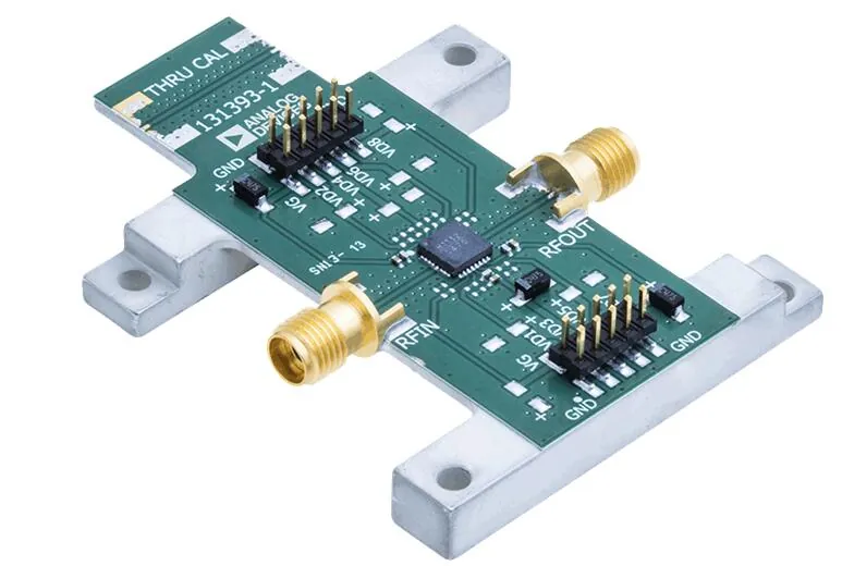
- MMICs consolidate multiple microwave functions onto a single semiconductor chip to reduce size and weight.
- The primary materials used in manufacturing include gallium arsenide (GaAs), gallium nitride (GaN), and silicon germanium (SiGe).
- These circuits are essential for high-frequency applications like 5G base stations, satellite communications, and automotive radar.
- Designers must account for parasitic effects and thermal management when developing high-power MMIC modules.
- Adopting MMIC technology significantly lowers assembly costs compared to traditional discrete, board-level microwave components.
What is a monolithic microwave integrated circuit?
The term “monolithic” refers to the fact that all active and passive components are fabricated on a single piece of semiconductor material. This construction method eliminates the need for wire bonds and interconnects between discrete parts, which are notorious for introducing signal loss and parasitic inductance at high frequencies. By integrating functions such as amplifiers, mixers, oscillators, and switches on one die, the monolithic microwave integrated circuit provides a highly reliable solution for complex signal processing.
Why use MMICs over discrete circuits?
The shift toward MMICs is driven by the need for smaller, more efficient systems. Discrete circuits suffer from significant signal degradation when components are physically separated by board traces. In contrast, the internal structure of an MMIC keeps signal paths extremely short. This architecture minimizes signal transition loss and allows for consistent, repeatable performance across large production volumes. Furthermore, the Federal Communications Commission regulates the power output of these devices to ensure safe operation in crowded spectral environments.
Common Semiconductor Materials
The selection of the substrate material dictates the electrical characteristics and power handling capabilities of the final circuit. Each material offers specific advantages depending on the application environment.
| Material Type | Primary Benefit | Typical Application |
|---|---|---|
| Gallium Arsenide | High electron mobility | Low-noise amplifiers |
| Gallium Nitride | High power density | Radar transmitters |
| Silicon Germanium | Cost-effective integration | Consumer wireless devices |
| Indium Phosphide | Extremely high frequency | Terahertz sensing systems |
Key Components in MMICs
Every MMIC is essentially a collection of specialized building blocks designed to handle specific tasks within the microwave signal chain. Passive components are just as critical as active transistors in these architectures.
Active and Passive Elements
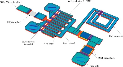
- Field-effect transistors (FETs): These act as the primary amplifying elements, often using high-electron-mobility transistor structures to handle rapid switching speeds.
- Thin-film resistors: Used for impedance matching and biasing circuits, these are deposited directly onto the substrate during the fabrication process.
- MIM Capacitors: Metal-insulator-metal capacitors provide the necessary decoupling and coupling functions required to maintain signal integrity.
- Spiral Inductors: These are integrated as planar structures on the semiconductor die, serving as essential components for tuning and filtering.
Design Challenges and Constraints
Designing an MMIC is significantly more complex than designing a standard low-frequency integrated circuit. The high frequency of operation means that even microscopic variations in the layout can lead to massive performance failures.
Pro Tip: Electromagnetic simulation software is absolutely vital during the design phase to predict how the physical geometry of the circuit traces will interact with the high-frequency electromagnetic fields.
Managing Thermal Dissipation
Because MMICs are so compact, they generate a high amount of heat in a very small area. If this heat isn’t properly managed, the semiconductor junction will reach temperatures that cause degradation or total failure. Engineers typically use thermal vias—small holes filled with conductive material—to draw heat away from the active transistors and into the base of the package or the heat sink.
Applications in Modern Technology
MMICs are found in almost every system that transmits or receives data at microwave frequencies. Without this technology, the modern world of mobile connectivity and high-speed radar would be physically impossible to build at a mass-production scale.
- 5G Telecommunications: High-frequency base stations require compact, high-efficiency power amplifiers that only MMIC technology can provide.
- Automotive Radar: Self-driving features depend on 77 GHz radar sensors, which utilize MMICs to detect obstacles with high precision in real-time.
- Satellite Communications: Space-grade MMICs are prized for their low weight and ability to withstand the harsh radiation environments of orbital flight.
- Defense Systems: Phased-array radar systems use thousands of tiny MMIC modules to steer beams electronically without moving parts.
Manufacturing and Fabrication Processes
The fabrication of an MMIC takes place in a cleanroom environment, involving a series of photolithography, etching, and deposition steps. The precision required is measured in nanometers, ensuring that every gate and contact is perfectly aligned.
The Fabrication Workflow
- Substrate Preparation: A high-purity wafer, such as GaAs, is polished and cleaned to serve as the foundation.
- Epitaxial Growth: Layers of semiconductor material are grown on the wafer to create the transistor channels.
- Photolithography: Patterns for the circuits are exposed onto the wafer using ultraviolet light.
- Metallization: Gold or other conductive metals are deposited to form the connections and passive components.
- Dicing: The wafer is cut into individual chips, which are then tested and packaged for final use.
Testing and Quality Assurance
Since internal connections can’t be probed directly once the chip is packaged, testing must be exhaustive during the wafer phase. Automated testing equipment uses specialized probes to measure the S-parameters, or scattering parameters, of every single circuit. These parameters describe how the MMIC handles signal reflection and transmission, confirming that the device meets the design specifications before it’s ever placed into a larger system.
Warning: Electrostatic discharge (ESD) is a major threat to MMIC components during handling; always utilize grounded workstations and anti-static wrist straps to prevent permanent damage to sensitive gate structures.
Future Trends in MMICs
The field is currently moving toward higher levels of integration and the use of even more exotic semiconductor materials. As the industry pushes toward 6G and beyond, the demand for circuits that can operate at frequencies above 100 GHz is skyrocketing.
- System-on-Chip (SoC) Integration: Combining digital processing and microwave front-ends on a single chip.
- Wide-Bandgap Materials: Ongoing research into diamond-based substrates to achieve unmatched thermal conductivity.
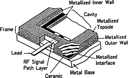
- Advanced Packaging: Moving from traditional wire-bonded packages to flip-chip and wafer-level packaging to further reduce parasitic losses.
Related guides
- Best Microwaves Under 200: Top 10 Picks for Every Need in 2026
- Oven vs Microwave Which Is Better for Your Cooking Needs in 2026
- Heating Food in Microwave Side Effects: The Scientific Truth in 2026
Frequently Asked Questions
What is the difference between an MMIC and an RFIC?
While the terms are sometimes used interchangeably, an RFIC (Radio Frequency Integrated Circuit) usually refers to circuits operating at lower RF frequencies, often using silicon-based processes like CMOS. An MMIC specifically targets the microwave and millimeter-wave spectrum, utilizing specialized semiconductor materials like GaAs or GaN to handle the unique physical demands of high-frequency signal propagation that standard silicon processes struggle to support.
Are MMICs expensive to produce?
Initial development costs for MMICs are high due to the specialized cleanroom equipment and design software required. However, once the design is finalized, the cost per unit drops significantly during mass production. For low-volume prototyping, the cost can range from $500 to $5,000 per wafer, but high-volume fabrication leverages economies of scale to make them viable for consumer electronics and automotive applications.
Can an MMIC be repaired if it fails?
No, an MMIC can’t be repaired. Because the components are integrated at the microscopic level on a semiconductor die, any physical damage or electrical burnout is permanent. If an MMIC fails, the standard industry procedure is to replace the entire chip. This is why strict quality control and thermal management during the initial design and integration phases are so critical to long-term system reliability.
How do I select the right MMIC for my project?
You must first define your operating frequency, required gain, and power output requirements. Once these parameters are set, you should consult the manufacturer’s datasheet for the S-parameters and thermal resistance ratings. It’s also important to consider the supply voltage and the availability of evaluation boards, which allow you to test the chip’s performance in a controlled environment before committing to a final PCB design.
What is the typical lifespan of an MMIC?
The lifespan of an MMIC is largely determined by its operating temperature and the power density of the transistors. When operated within the manufacturer’s specified thermal limits, high-quality MMICs can last for hundreds of thousands of hours. In harsh environments like aerospace or automotive engine bays, designers often implement active thermal monitoring to ensure the device doesn’t exceed its rated junction temperature, thereby extending the overall operational life.
Conclusion
Selecting the right monolithic microwave integrated circuit requires balancing your specific frequency requirements with the thermal and power constraints of your application. Begin your design process by reviewing the technical specifications provided by reputable semiconductor manufacturers to ensure compatibility with your system architecture. Incorporate thorough electromagnetic simulations early in your development cycle to avoid costly design iterations and ensure your project meets its performance targets reliably.
